- 您现在的位置:买卖IC网 > Sheet目录3861 > PIC18F26K80-I/MM (Microchip Technology)MCU PIC 64KB FLASH 28QFN
2010-2012 Microchip Technology Inc.
DS39977F-page 187
PIC18F66K80 FAMILY
11.6
PORTE, TRISE and
LATE Registers
PORTE is a seven-bit-wide, bidirectional port. The
corresponding Data Direction and Output Latch registers
are TRISE and LATE.
All pins on PORTE are implemented with Schmitt
Trigger input buffers. Each pin is individually
configurable as an input or output.
Each of the PORTE pins has a weak internal pull-up. A
single control bit can turn off all the pull-ups. This is
performed by clearing bit, REPU (PADCFG1<6>). The
weak pull-up is automatically turned off when the port
pin is configured as an output. The pull-ups are
disabled on any device Reset.
PORTE is also multiplexed with the Parallel Slave Port
address lines. RE1 and RE0 are multiplexed with the
Parallel Slave Port (PSP) control signals, WR and RD.
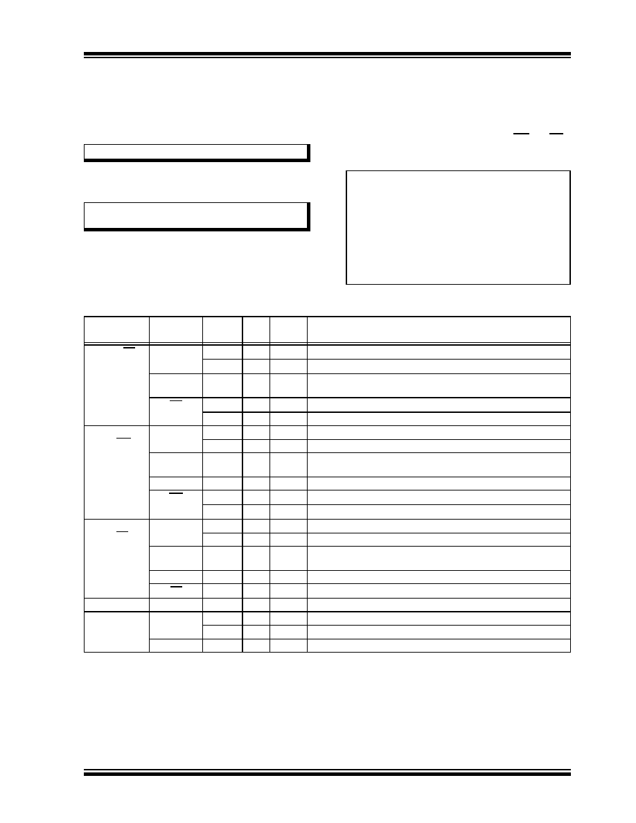
EXAMPLE 11-5:
INITIALIZING PORTE
Note:
PORTE is unavailable on 28-pin devices.
Note:
These pins are configured as digital inputs
on any device Reset.
CLRF
PORTE
; Initialize PORTE by
; clearing output
; data latches
CLRF
LATE
; Alternate method
; to clear output
; data latches
MOVLW
03h
; Value used to
; initialize data
; direction
MOVWF
TRISE
; Set RE<1:0> as inputs
; RE<7:2> as outputs
TABLE 11-9:
PORTE FUNCTIONS
Pin Name
Function
TRIS
Setting
I/O
I/O Type
Description
RE0/AN5/RD
RE0
0
O
DIG
LATE<0> data output.
1
I
ST
PORTE<0> data input.
AN5
1
I
ANA
A/D Input Channel 5. Default input configuration on POR; does not
affect digital output.
RD
x
O
DIG
Parallel Slave Port read strobe pin.
x
I
ST
Parallel Slave Port read pin.
RE1/AN6/
C1OUT/WR
RE1
0
O
DIG
LATE<1> data output.
1
I
ST
PORTE<1> data input.
AN6
1
I
ANA
A/D Input Channel 5. Default input configuration on POR; does not
affect digital output.
C1OUT
0
O
DIG
Comparator 1 output; takes priority over port data.
WR
x
O
DIG
Parallel Slave Port write strobe pin.
x
I
ST
Parallel Slave Port write pin.
RE2/AN7/
C2OUT/CS
RE2
0
O
DIG
LATE<2> data output.
1
I
ST
PORTE<2> data input.
AN7
1
I
ANA
A/D Input Channel 7. Default input configuration on POR; does not
affect digital output.
C2OUT
0
O
DIG
Comparator 2 output; takes priority over port data.
CS
x
I
ST
Parallel Slave Port chip select.
RE3
1
I
ST
PORT<3> data input.
RE4/CANRX
RE4(1)
0
O
DIG
LATE<4> data output.
1
I
ST
PORTE<4> data input.
CANRX(1,2)
1
I
ST
CAN bus RX.
Legend:
O = Output, I = Input, ANA = Analog Signal, DIG = CMOS Output, ST = Schmitt Trigger Buffer Input,
x
= Don’t care (TRIS bit does not affect port direction or is overridden for this option)
Note
1:
These bits are unavailable for 40 and 44-pin devices (PIC18F4XK0).
2:
This is the alternate pin assignment for CANRX and CANTX on 64-pin devices (PIC18F6XK80) when the CANMX
Configuration bit is cleared.
发布紧急采购,3分钟左右您将得到回复。
相关PDF资料
PIC16C55-RC/P
IC MCU OTP 512X12 28DIP
SFW23R-2STE1
SFW23R-2STE1-FFC/FPC CONN
PIC24FJ64GA002-E/SS
IC PIC MCU FLASH 64K 28-SSOP
PIC18LF46K22-I/ML
IC PIC MCU 64KB FLASH 44QFN
PIC18F45K80-I/ML
MCU PIC 32KB FLASH 44QFN
PIC24F32KA302-I/ML
MCU 32KB FLASH 2KB RAM 28-QFN
PIC18LF45K80-I/ML
MCU PIC ECAN 32KBFLASH 44QFN
PIC18F4221-I/PT
IC PIC MCU FLASH 2KX16 44TQFP
相关代理商/技术参数
PIC18F26K80-I/SO
功能描述:8位微控制器 -MCU 64KB FL 4KBRM 16MIPS 12bit ADC CTMU RoHS:否 制造商:Silicon Labs 核心:8051 处理器系列:C8051F39x 数据总线宽度:8 bit 最大时钟频率:50 MHz 程序存储器大小:16 KB 数据 RAM 大小:1 KB 片上 ADC:Yes 工作电源电压:1.8 V to 3.6 V 工作温度范围:- 40 C to + 105 C 封装 / 箱体:QFN-20 安装风格:SMD/SMT
PIC18F26K80-I/SP
功能描述:8位微控制器 -MCU 64KB FL 4KBRM 16MIPS 12bit ADC CTMU RoHS:否 制造商:Silicon Labs 核心:8051 处理器系列:C8051F39x 数据总线宽度:8 bit 最大时钟频率:50 MHz 程序存储器大小:16 KB 数据 RAM 大小:1 KB 片上 ADC:Yes 工作电源电压:1.8 V to 3.6 V 工作温度范围:- 40 C to + 105 C 封装 / 箱体:QFN-20 安装风格:SMD/SMT
PIC18F26K80-I/SS
功能描述:8位微控制器 -MCU 64KB FL 4KBRM 16MIPS 12bit ADC CTMU RoHS:否 制造商:Silicon Labs 核心:8051 处理器系列:C8051F39x 数据总线宽度:8 bit 最大时钟频率:50 MHz 程序存储器大小:16 KB 数据 RAM 大小:1 KB 片上 ADC:Yes 工作电源电压:1.8 V to 3.6 V 工作温度范围:- 40 C to + 105 C 封装 / 箱体:QFN-20 安装风格:SMD/SMT
PIC18F26K80T-I/ML
功能描述:8位微控制器 -MCU 64KB FL 4KBRM 16MIPS 12bit ADC CTMU RoHS:否 制造商:Silicon Labs 核心:8051 处理器系列:C8051F39x 数据总线宽度:8 bit 最大时钟频率:50 MHz 程序存储器大小:16 KB 数据 RAM 大小:1 KB 片上 ADC:Yes 工作电源电压:1.8 V to 3.6 V 工作温度范围:- 40 C to + 105 C 封装 / 箱体:QFN-20 安装风格:SMD/SMT
PIC18F26K80T-I/MM
功能描述:8位微控制器 -MCU ECAN 64KB FL 4KBRM 16 MIPS 12b ADC CTMU RoHS:否 制造商:Silicon Labs 核心:8051 处理器系列:C8051F39x 数据总线宽度:8 bit 最大时钟频率:50 MHz 程序存储器大小:16 KB 数据 RAM 大小:1 KB 片上 ADC:Yes 工作电源电压:1.8 V to 3.6 V 工作温度范围:- 40 C to + 105 C 封装 / 箱体:QFN-20 安装风格:SMD/SMT
PIC18F26K80T-I/SO
功能描述:8位微控制器 -MCU 64KB FL 4KBRM 16MIPS 12bit ADC CTMU RoHS:否 制造商:Silicon Labs 核心:8051 处理器系列:C8051F39x 数据总线宽度:8 bit 最大时钟频率:50 MHz 程序存储器大小:16 KB 数据 RAM 大小:1 KB 片上 ADC:Yes 工作电源电压:1.8 V to 3.6 V 工作温度范围:- 40 C to + 105 C 封装 / 箱体:QFN-20 安装风格:SMD/SMT
PIC18F26K80T-I/SS
功能描述:8位微控制器 -MCU 64KB FL 4KBRM 16MIPS 12bit ADC CTMU RoHS:否 制造商:Silicon Labs 核心:8051 处理器系列:C8051F39x 数据总线宽度:8 bit 最大时钟频率:50 MHz 程序存储器大小:16 KB 数据 RAM 大小:1 KB 片上 ADC:Yes 工作电源电压:1.8 V to 3.6 V 工作温度范围:- 40 C to + 105 C 封装 / 箱体:QFN-20 安装风格:SMD/SMT
PIC18F27J13-I/ML
功能描述:8位微控制器 -MCU 128KB Flash 4KB RAM 12MIPS nanoWatt RoHS:否 制造商:Silicon Labs 核心:8051 处理器系列:C8051F39x 数据总线宽度:8 bit 最大时钟频率:50 MHz 程序存储器大小:16 KB 数据 RAM 大小:1 KB 片上 ADC:Yes 工作电源电压:1.8 V to 3.6 V 工作温度范围:- 40 C to + 105 C 封装 / 箱体:QFN-20 安装风格:SMD/SMT